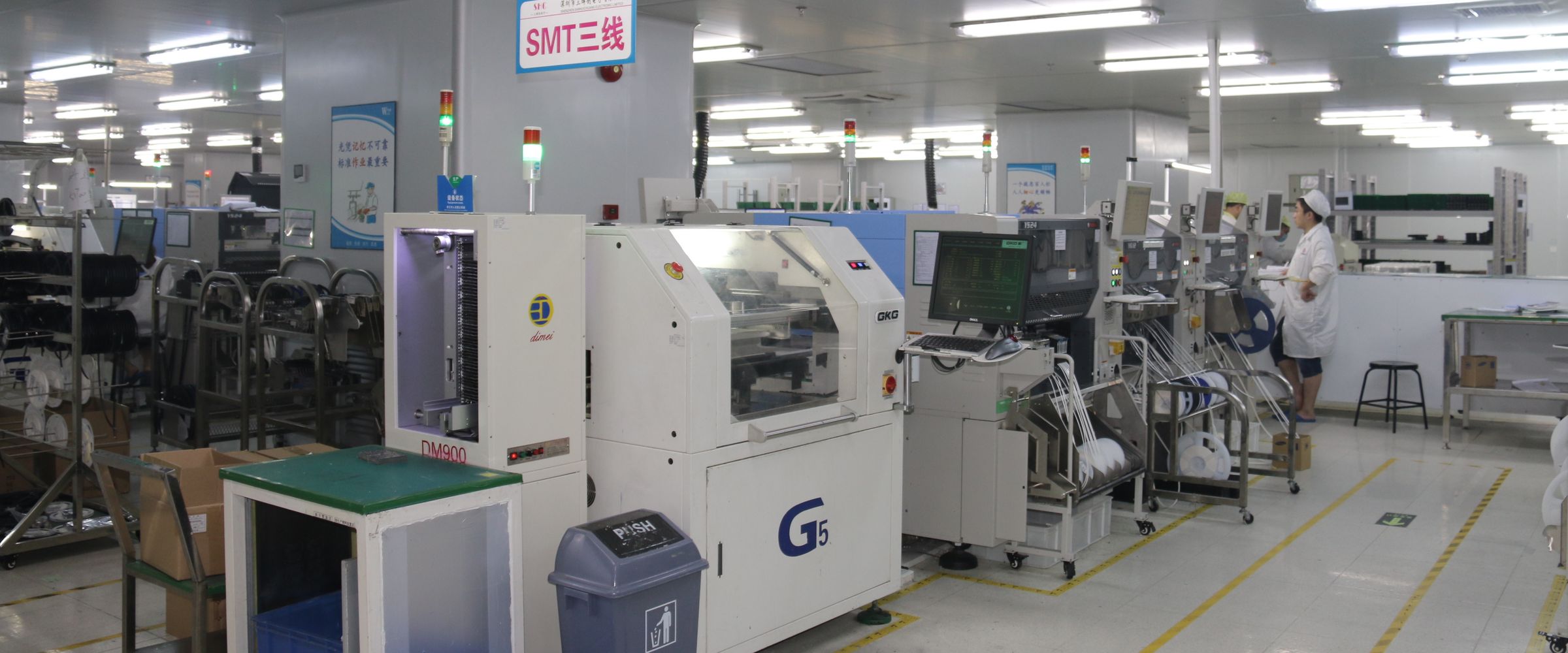
Everything below is a real production figure from our Shenzhen factory — not a marketing claim. If a number you need is missing, ask us and we will confirm it.
The limits that decide whether your design can be built here.
| SMT production lines | 24 |
| DIP (through-hole) assembly lines | 6 |
| Smallest component package | 01005 |
| Largest component package | 2512 |
| BGA minimum pitch | 0.3 mm – 1.25 mm |
| Maximum PCB size | 450 mm × 470 mm |
| Minimum order quantity | 1 piece |
| PCB fabrication — layer count | 1 – 32 layers |
| PCB fabrication — minimum line / space | 0.06 mm / 0.06 mm |
| PCB fabrication — maximum board size | 650 mm × 1,100 mm |
Note the two different limits: a bare board can be fabricated up to 650 × 1,100 mm, but a board that goes through SMT assembly is limited to 450 × 470 mm. If your design is larger than the assembly limit, it has to be split across a panel — tell us before you order and we will confirm how.
RigidFlexibleRigid-flex
The largest single board we can fabricate, in 1 to 32 layers, on FR4, Rogers, Taconic, aluminium or high-TG laminate.
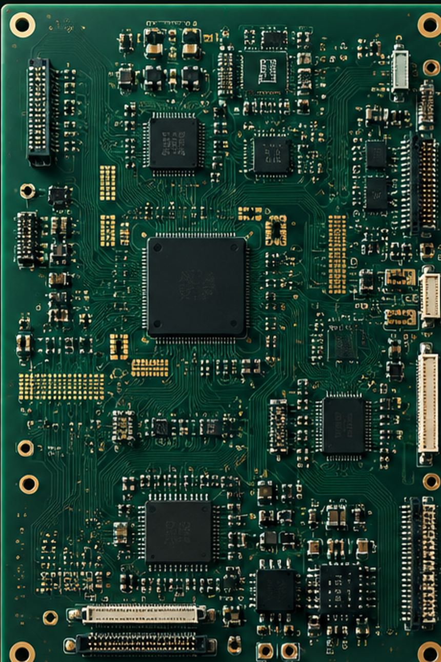
Assembly is the tighter of the two limits. A board built at the full fabrication size carries 3.4 times the area this line will take.
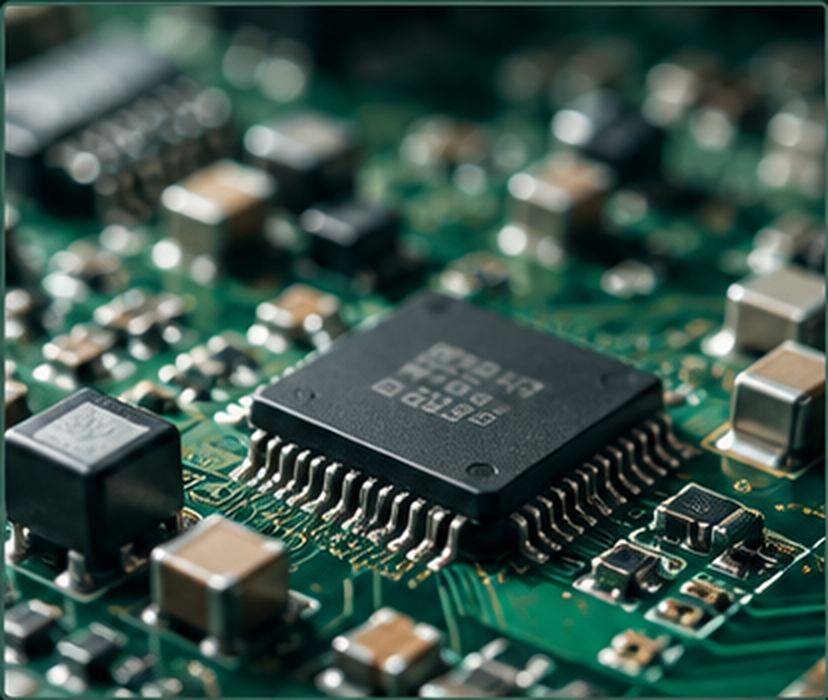
A board larger than this must be split across a panel. Tell us before you order and we will confirm how.
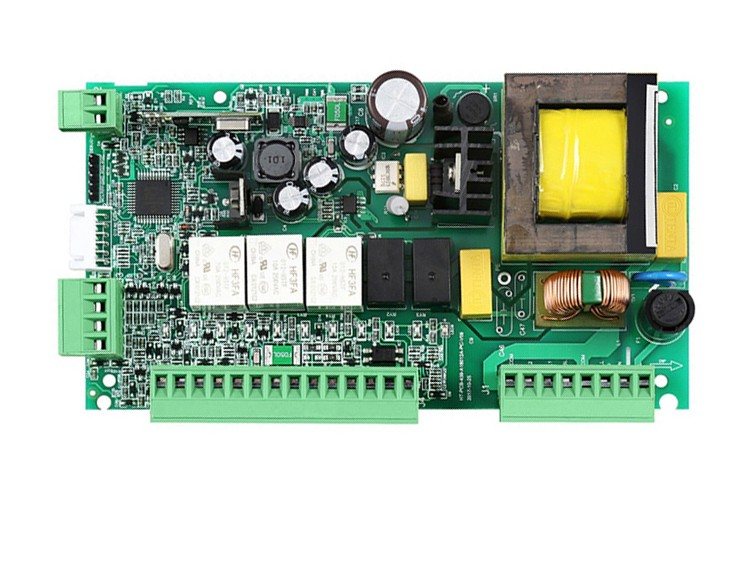
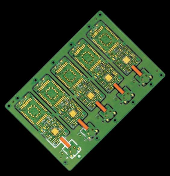
Three of the boards in this group, as they left the line. There is no caption saying what each one does — the part numbers on the chips are the only product names printed on them, and a customer's design is not ours to name.
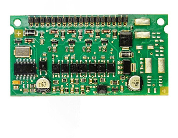
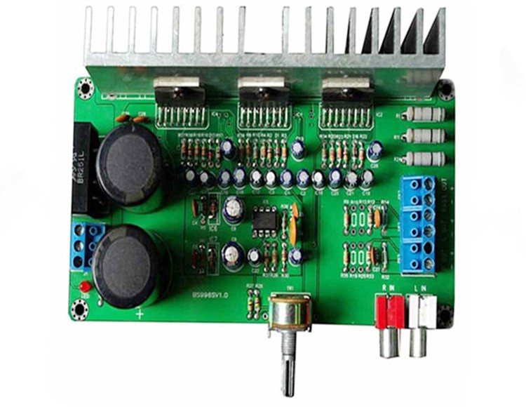
Daily output by line type. This is the section that tells you whether we can absorb your volume.
| Line type | Lines | Capacity per day |
|---|---|---|
| YAMAHA SMT | 13 | 27.17 million points |
| Panasonic SMT | 4 | 8.36 million points |
| JUKI SMT | 7 | 4.86 million points |
| Total SMT | 24 | 40.39 million points |
| Line | Count | Capacity per day |
|---|---|---|
| Plug-in (through-hole) lines | 4 | 800,000 points |
| Manual soldering lines | 3 | 200,000 points |
| 22-metre assembly lines | 3 | 15,000 units |
| Testing lines | 6 | 60,000 units |
| UV / polyurethane conformal coating | 10 | 100,000 pieces sprayed |
| Automatic dispensing | 3 | 30,000 pcs |
| Automatic board separation | 7 | 100,000 pcs |
| PECVD coating equipment | 2 | 20,000 pcs |
The full fabrication capability, including flexible and rigid-flex. Everything a PCB-only buyer needs, on one page.
| Layer count | 1 – 32 layers |
| Base material | FR4, CEM1, CEM3, High TG, Rogers, F4B, Taconic, FR1, FR2, 94V0, aluminium |
| Board type | Rigid, flexible, rigid-flexible, HDI |
| Board shape | Rectangular, round, slots, cutouts, complex, irregular |
| Board cutting | Shear, V-score, tab-routed, countersunk |
| Order quantity | 1 – 500,000 |
| Production lead time | Prototype 3–4 days; mass production 8–16 days |
| Board thickness | 0.2 – 8.0 mm (flex: 0.01 – 0.25 in) |
| Copper weight | 0.5 oz – 12 oz |
| Minimum line width / spacing | 0.06 mm / 0.06 mm |
| Maximum board dimensions | 650 mm × 1,100 mm (25.6 in × 43.3 in) |
| Minimum drill hole diameter | 0.1 mm |
| Minimum laser-drilled hole | 0.075 mm |
| Minimum slot width | 3.0 mm (0.12 in / 120 mil) |
| Solder mask | Double-sided green LPI as standard; red, white, yellow, blue, black and purple available |
| Silkscreen | Single- or double-sided, in white, yellow, black, or negative |
| Surface finish | HASL, ENIG, immersion tin, immersion silver, OSP, ENEPIG, electrolytic hard gold, gold fingers, ENIG + OSP |
| Special processes | Half holes, bonding, impedance control, metal cladding, resin plug holes, blue glue, carbon ink, blind routing, blind and buried vias |
| Board thickness tolerance | ± 10% |
| V-score depth | 20–25% of board thickness |
| PTH wall thickness | > 0.025 mm |
| PTH hole diameter tolerance | ± 0.076 mm |
| NPTH hole diameter tolerance | ± 0.05 mm |
| Hole position deviation | ± 0.076 mm |
| Countersunk holes | Yes |
| Quality standard | IPC-A-600F / MIL-STD-105D |
| Design files accepted | Gerber RS-274X and 274D, KiCad, Eagle, Altium/Pro-E, AutoCAD DXF and DWG |
Production lead time depends on the board type, layer count, surface finish and quantity. Read the row above as the range our fabrication runs at, not as a promise for a specific design. A board that also has components placed on it is scheduled differently — see where PCBA lead time actually goes.
Inspection is where an assembly line either earns its reputation or loses it.
Seven steps, in this order. A defect that is not caught at step 2 becomes expensive by step 6.
What we run, and how much of it.
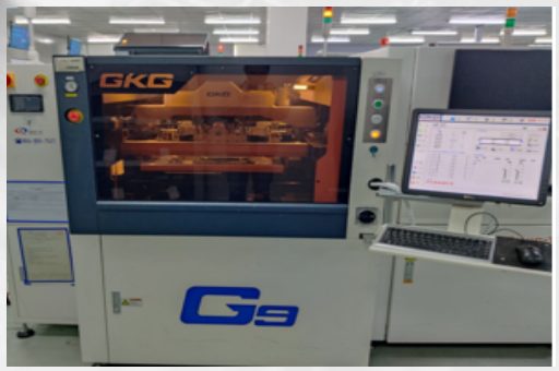
24 automatic printing machines, with 3D SPI (solder paste inspection) — 8 units.
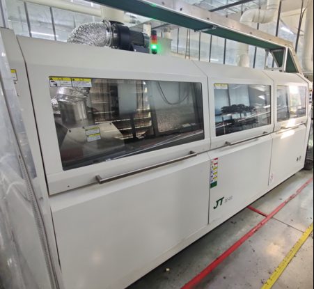
10 hot-air reflow ovens and 4 wave soldering machines.
20 offline AOI and 6 in-line AOI systems, including 3D AOI.
3D X-ray for BGA and hidden-joint inspection.
1 BGA rework station and 1 laser cutting machine.
4 FAI devices — the check that catches a problem before 10,000 boards have it.
The machines actually used to build your board. If you are evaluating suppliers at a distance, ask for these shots in a video call — and ask for the machine IDs on the screens.
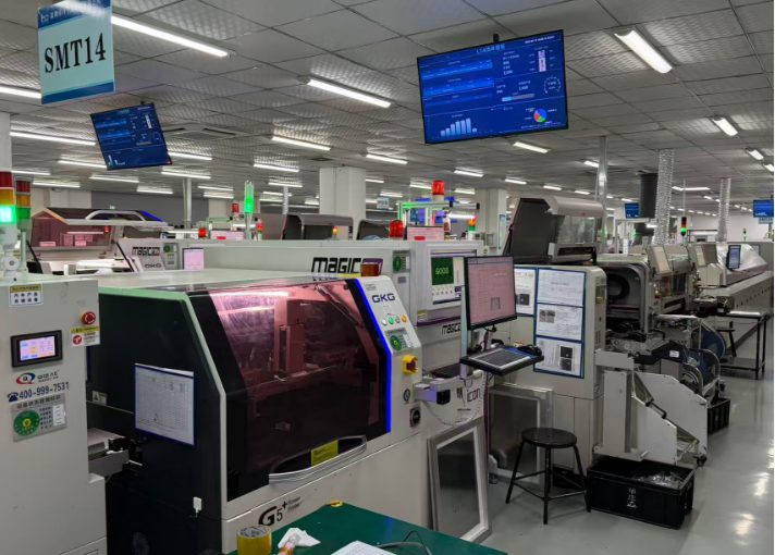
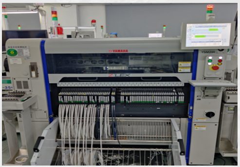
You are not coordinating five suppliers for one product.
Electronic and industrial design support, before manufacturing starts.
PCB and FPC manufacturing from your Gerber files.
Metal and plastic parts, so the finished product ships complete.
Component sourcing from Sharp, Toshiba, STMicroelectronics, Samsung, Infineon, JRC and NEC — plus replacement solutions for obsolete parts.
SMT, DIP and manual soldering, with testing before shipment.
IATF 16949, ISO 13485, ISO 9001 and IPC-A-610 Class III.
Send us the Gerber files and BOM. We will confirm what we can build, flag anything that will cause a problem on the line, and come back with a price within 24 hours.